🛒 Best Price Today on Amazon
Prime members get fast, free shipping on everything above, plus member-only deals. New members get a 30-day free trial — cancel anytime.
A graphics card’s specifications reveal more than clock speeds and VRAM. Understanding gpu die size explained helps you see how much physical silicon sits inside a GPU, how chip design affects manufacturing, and why larger chips are not automatically faster. This guide breaks down die area, transistor density, chiplets, and their practical importance for PC gaming.
What GPU Die Size Really Comes Down To
GPU die size measures the physical area of the silicon chip containing the graphics processor’s circuitry. Manufacturers and hardware databases typically express this measurement in square millimeters (mm²). It provides useful information about chip complexity and manufacturing, but it does not independently determine gaming performance. To understand its significance, you need to consider architecture, transistor density, and manufacturing technology together.
1. What Is a GPU Die?
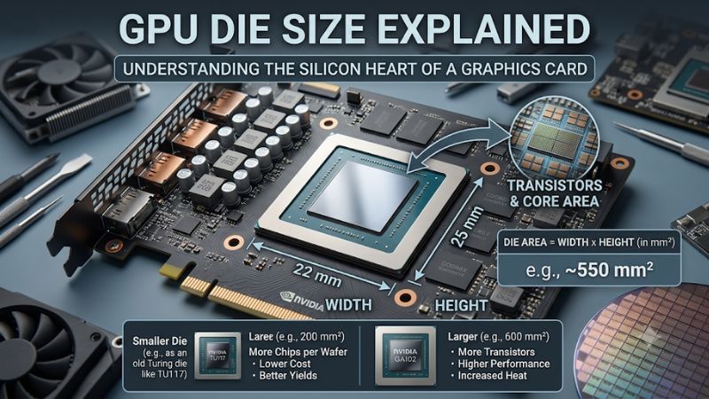
A GPU die is the actual piece of semiconductor silicon containing the processing circuitry. It houses components such as shader cores, memory controllers, cache, ray-tracing hardware, and other functional units, depending on the GPU architecture.
During manufacturing, multiple chip designs are created on a silicon wafer. The wafer is then cut into individual dies, which are packaged to become usable semiconductor components. In a discrete graphics card, the GPU package is mounted on the PCB and connected to surrounding memory chips and other components.
When discussing gpu die size, the measurement refers to the silicon area of the graphics processor itself, not the entire graphics card. A large triple-fan graphics card can contain a relatively small GPU die because its physical dimensions are also determined by its cooler, PCB, power-delivery components, and memory configuration.
2. How Is GPU Die Size Measured?
GPU die area is measured in square millimeters (mm²). For example, a GPU with a die area of 300 mm² has a silicon surface area of 300 square millimeters. This is a measurement of area rather than the chip’s length, width, thickness, or overall package dimensions.
The distinction matters because a die is generally a rectangular piece of silicon, and its reported area does not reveal its exact dimensions. Two dies can have the same area while using different layouts, circuit arrangements, and manufacturing processes.
You may encounter this specification in GPU databases, semiconductor architecture documentation, and hardware identification utilities such as GPU-Z. If a database does not provide the value, it is better to treat it as unavailable than estimate it from a photograph or graphics card dimensions.
3. What Is the Relationship Between Die Size and Transistor Count?
Transistors are the fundamental electronic switches used to perform calculations and control data movement inside a GPU. More transistors can support additional processing units, larger caches, and more complex functionality, although the actual implementation depends on the architecture.
A larger die can accommodate more transistors, but this relationship is not automatic. A newer manufacturing process can fit more transistors into a smaller area. This is why a newer GPU may have more transistors than an older model without having a proportionally larger silicon die.
Transistor density helps explain the difference. It describes how many transistors are integrated into a given area. Comparing transistor count alongside die area provides a more useful picture of chip complexity than looking at physical size alone.
4. Does a Smaller Manufacturing Process Mean a Smaller GPU Die?
Manufacturing process technology influences how densely transistors can be integrated into a semiconductor. You will commonly see terms such as 5nm, 6nm, 7nm, and 8nm in GPU specifications and architecture discussions.
A more advanced process can potentially accommodate more circuitry within a particular area. However, manufacturers may use those density improvements to add more processing units, larger caches, or additional functionality rather than reducing the die’s overall dimensions.
It is also important to understand that modern process-node labels are not literal measurements of every transistor’s physical dimensions. Different foundries use different naming conventions and design technologies, so comparing node numbers across manufacturers does not provide a complete picture of actual transistor density.
How GPU Die Size Affects Performance and Manufacturing
Understanding gpu die size becomes more useful when you connect silicon area with manufacturing economics and graphics architecture. A large chip can provide room for more processing resources, but its performance depends on how those resources are designed, powered, and utilized. Manufacturing yield, thermal characteristics, and multi-die packaging also influence how GPU manufacturers develop their products.
1. Why Do Larger GPU Dies Cost More to Manufacture?
Larger dies generally create manufacturing challenges because fewer individual chips can fit onto a single silicon wafer. They are also more exposed to the possibility that a manufacturing defect will affect part of the functional circuitry.
This can reduce manufacturing yield, meaning a smaller percentage of fabricated dies become usable products. The effect depends on the manufacturing process, defect density, chip design, and production conditions.
However, die area is not the only factor determining the final price of a graphics card. Packaging, memory, PCB components, cooling, research and development, manufacturing capacity, and market demand also contribute to its cost.
2. Does a Larger Die Mean Better Gaming Performance?
Not necessarily. A larger GPU die can accommodate more hardware resources, but the amount of usable processing power depends on the architecture and how efficiently the chip executes graphics workloads.
For gaming, performance also depends on shader throughput, clock speeds, memory bandwidth, cache, VRAM capacity, driver optimization, and the game itself. A smaller GPU built on a newer process can outperform a larger older chip because of architectural improvements and higher operating efficiency.
This is why comparing two graphics cards using die area alone can lead to misleading conclusions. A GPU with a larger silicon footprint is not automatically the better choice for 1440p gaming, 4K gaming, or ray tracing.
3. How Do Chiplets Change GPU Die Size?
Traditional monolithic GPU designs place the main processing circuitry on one large silicon die. Chiplet designs divide certain functions across multiple smaller dies that communicate within the same package.
AMD demonstrated this approach with its RDNA 3 architecture in the Radeon RX 7900 series. Its design uses a 5nm Graphics Compute Die (GCD) measuring 306 mm² alongside six 6nm Memory Cache Dies (MCDs), each measuring 37.5 mm².
This distinction is important when interpreting specifications. Looking only at the main compute die does not describe the complete silicon configuration of a multi-die GPU. You must account for the additional dies when comparing package architectures or discussing total silicon area.
Chiplets also provide manufacturers with greater flexibility when combining different manufacturing processes. However, communication between dies introduces additional design and packaging considerations.
4. How Does Die Size Relate to Heat and Power Consumption?
A GPU die contains billions of transistors switching at high speeds during demanding workloads. These operations consume electrical power and generate heat, which must be transferred through the chip package and cooling system.
A larger die does not automatically produce more heat. Total power consumption depends on the architecture, voltage, clock frequency, transistor characteristics, workload, and power-management behavior.
Thermal density is another important consideration. Two GPUs with similar power consumption can distribute heat differently across their silicon surfaces. A smaller area with concentrated power consumption can create different cooling challenges from a larger area with a more distributed workload.
For gamers, the practical takeaway is to examine actual GPU power specifications, temperatures, cooling design, and performance measurements rather than treating die area as a direct indicator of operating temperature.
GPU Die Size vs. Other Important GPU Specifications
The following table explains how die area differs from the specifications commonly used when comparing gaming graphics cards.
| Specification | What It Measures | Why It Matters |
| Die Size | Physical silicon area in mm² | Indicates chip area and helps explain manufacturing complexity |
| Transistor Count | Number of transistors | Provides insight into chip complexity |
| Transistor Density | Transistors per unit of area | Helps compare silicon integration |
| Process Node | Semiconductor manufacturing technology designation | Provides manufacturing context |
| VRAM Capacity | Dedicated graphics memory | Determines how much graphics data can reside in memory |
| Memory Bandwidth | Data transfer capacity per second | Affects how quickly the GPU can access external memory |
| Core Count | Architecture-specific processing units | Helps describe available processing resources |
| TDP/TGP | Defined thermal or graphics power rating | Helps with power and cooling planning |
These specifications describe different aspects of a graphics card. For example, VRAM capacity tells you how much dedicated memory is available, while die size describes the silicon area of the processor.
When choosing a gaming GPU, prioritize independent gaming benchmarks, VRAM requirements, power consumption, and compatibility. Die area is useful supporting information, not a standalone buying metric.
How to Check and Interpret GPU Die Size: Step by Step
You can find and interpret this specification without opening your graphics card or modifying its hardware. The process involves identifying your exact GPU model, locating a reliable specification database, and comparing die area with other architectural information. These steps are particularly useful when researching older graphics cards or comparing different GPU generations.
Step 1: Identify Your Exact Graphics Card Model
Start by identifying the graphics card installed in your computer. On Windows, open Task Manager using Ctrl + Shift + Esc, select Performance, and choose GPU from the sidebar.
You can also open Device Manager, expand Display adapters, and check the detected graphics hardware. Record the complete model name rather than relying on a general family name such as GeForce RTX 50 Series or Radeon RX 9000 Series.
This distinction matters because different GPUs within the same generation can use different silicon designs, transistor counts, and die areas. Laptop and desktop versions may also have different configurations.
Step 2: Find the Die Size Specification
Once you have the exact GPU model, look for its die area in a reputable hardware database or the manufacturer’s architecture documentation.
GPU-Z can also provide useful hardware identification information. Open its Graphics Card tab and inspect the available specifications. Depending on the GPU and available database information, the Die Size field may be populated or unavailable.
Do not assume every field is directly measured by the utility. Some specifications are database-derived, so verify important figures against manufacturer documentation or reliable semiconductor references.
Step 3: Compare Die Area With Transistor Density
After locating the measurement, compare it with transistor count and manufacturing technology. This helps explain whether a GPU uses a relatively large silicon area because of its overall design or because its architecture integrates more circuitry per square millimeter.
You can calculate approximate transistor density using:
TransistorDensity=TransistorCountDieArea
For example, if a hypothetical GPU contains 30 billion transistors across a 300 mm² die:
30,000300=100
The result is approximately 100 million transistors per mm².
This calculation is useful for understanding semiconductor integration, but it does not measure gaming performance or indicate how efficiently those transistors are used.
Step 4: Evaluate the GPU Using Real Gaming Specifications
Finally, compare the GPU’s actual gaming capabilities rather than making a purchasing decision based on silicon area. Check independent benchmarks at your intended resolution and graphics settings.
Pay particular attention to average FPS, 1% lows when available, VRAM capacity, ray-tracing performance, power consumption, and upscaling support. Keep benchmark results from different test systems and game versions separate.
If you are comparing two graphics cards, use results from the same benchmark source and comparable test conditions whenever possible. This gives you a much more reliable understanding of their gaming performance than comparing die dimensions.
Common Mistakes When Reading GPU Die Specifications
Avoid these common misunderstandings when researching graphics hardware:
- Confusing die size with graphics card dimensions: Die area measures the processor’s silicon, not the length or thickness of the complete card.
- Assuming larger means faster: Architecture, clock speeds, and available processing resources determine how effectively the GPU performs.
- Treating process-node numbers as exact transistor dimensions: Node labels are manufacturing designations, not literal measurements of every transistor.
- Ignoring chiplet configurations: A multi-die GPU can have additional silicon beyond its main compute die.
- Using die area as a thermal rating: Power consumption, thermal density, and cooling design provide more useful thermal information.
- Comparing transistor counts without context: Different architectures can use their transistors for different functions.
Frequently Asked Questions
1. Is a Bigger GPU Die Always Better?
No, a bigger GPU die is not always better. More silicon area can accommodate additional processing resources, but gaming performance depends on architecture, clock speeds, memory systems, and workload optimization. A smaller, newer GPU can outperform a larger older model.
2. Does GPU Die Size Affect FPS?
GPU die size does not directly determine FPS. It can indirectly influence the amount of hardware that fits inside a processor, but actual frame rates depend on processing capabilities, memory performance, game optimization, and graphics settings. Independent benchmarks provide a better comparison.
3. Can I Check GPU Die Size Without Removing My Graphics Card?
Yes, you can check reported GPU specifications using GPU-Z or a reliable online GPU database. Look for the Die Size field or the manufacturer’s architecture documentation. You do not need to remove the graphics card or open its cooler.
4. Is GPU Die Size the Same as VRAM Capacity?
No, GPU die size and VRAM capacity measure completely different things. Die size describes the physical area of the GPU’s silicon processor in mm², while VRAM capacity measures dedicated graphics memory in GB. Both matter to GPU design, but they serve different purposes.
Final Thoughts
Understanding gpu die size helps explain how graphics processors are designed, manufactured, and packaged. However, silicon area alone cannot tell you whether a graphics card delivers better gaming performance or value. When comparing GPUs, use die size as supporting technical information and prioritize independent benchmarks, architecture, VRAM, and power requirements.